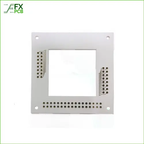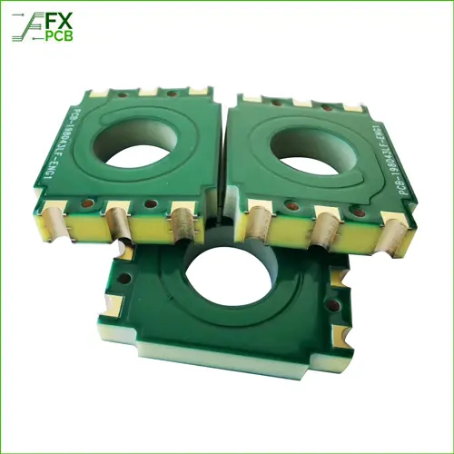
Thick Film Ceramic PCB

Thick film ceramic PCB is a circuit board made by screen-printing metal wiring layers onto ceramic bases, which are then solidified through high-temperature sintering. It is widely used in auomotive electronics and other fields where high circuit precision required are not so high, and the manufacturing process is simple, low cost and excellent thermal shock resistance.


Description

Ceramic PCB Materials Properties:

ItemUnitValueTest Standard
Color/Gray3.2
Densityg/cm³≥ 3.33GB/T 2413
Thermal Conductivity20℃, W/(m · K)≥ 170GB/T 5598
Dielectric Constant1MHz8~10GB/T 5594.4
Dielectric StrengthKV/mm≥ 17GB/T 5593
Flexural StrengthMpa≥ 450GB/T 5593
CamberLength‰≤2‰
Surface Roughness Raµ m0.3~0.6GB/T 6062
Water Absorption%0GB/T 3299—1996
Volume Resistivity20℃, Ω .cm≥ 10¹³GB/T 5594.5
Thermal Expansion10-6 mm      20~300℃2~3GB/T 5593


FX PCB use the ceramic material imported from Germany and Fujian Huaqing, all incoming material will be strictly checked for the material properties. See the capability of FX PCB for the Ceramic.

Ceramic PCB Capability:

Board Thickness(mm)       0.25/0.38/0.5/0.635/1.0/1.5/2.0/2.5/3.0mm
Layer Number     1-2L
Base copper thickness(um)18-300um(0.5-8.5oz)
Min Track width/space(mm)  0.075mm
Min hole size0.06mm(PTH)
Finished hole tolerance(mm) 0.05mm(NPTH)
Outline Tolerance(mm)0.05mm
Hole Tolerance    +/-0.05mm
Min space from track to board edge0.2mm
 

Finished board thickness

(0.25-0.38mm)+/-0.03mm
(0.38-0.635)+/-0.04mm
(0.76-2mm)+/-0.05mm
Surface TreatmentENIG,ENEPIG,Immersion Silver
MaterialAIN, AI203