An IC substrate (IC carrier) is the bridge between a bare semiconductor die and the printed circuit board: it fans out the chip’s fine-pitch connections, carries power and signals, and protects the die. FX PCB manufactures custom IC substrate PCBs in Shenzhen, China — through-hole builds of 2–24 layers, HDI builds up to 10 layers / 4 stacks in production and 14 layers / 7 stacks for samples, with 35/35µm line width and spacing.
Send us your design files and stack-up requirements, and our engineers will review them and return a quote in 1–2 working days.
Applications
Our IC substrates are built for:
- High-end servers and data-center AI chips
- 5G base-station RF modules
- Smartphone AP / CPU packages
- High-end medical imaging equipment
- Automotive autonomous-driving domain controllers
Substrate Materials
- BT resin (black / white) — the mainstream substrate material for module, memory, and RF packages.
- FR-4 and halogen-free laminates
- PTFE (Teflon) and BTFE — for RF and high-frequency packages.
- High-frequency materials — full range available.
Process Capability
| Item | Capability |
|---|---|
| Materials | BT (black/white), FR-4, PTFE, BTFE, halogen-free, high-frequency materials |
| Layers | Through-hole 2–24 layers (sample & production); HDI production up to 10 layers / 4 stacks; HDI samples up to 14 layers / 7 stacks |
| Max. board size | 520 × 580 mm |
| Finished board thickness | 0.08–1.6 mm |
| Min. finished thickness tolerance | ±0.02 mm |
| Min. inner core thickness | 0.025 mm |
| Layer-to-layer registration | ±0.02 mm |
| Circuit copper thickness | 8–70 µm |
| Min. line width / space (inner & outer) | 35 / 35 µm |
| Min. finished hole | 0.070 mm (mechanical) / 0.035 mm (laser) |
| Drill size range | 0.07–6.50 mm |
| Finished hole tolerance | ±0.025 mm (PTH / NPTH) |
| Hole position accuracy | ±0.02 mm |
| Hole copper thickness | 10–250 µm |
| Max. aspect ratio | 25:1 |
| Impedance tolerance | ±8% |
| Min. solder mask opening | 2 mil |
| Min. solder mask dam | 2 mil |
| Min. circuit dimension tolerance | ±5 µm |
| Outline tolerance | ±0.05 mm (2 mil) |
| Profiling | CNC routing, automatic large-panel V-cut, die punching, laser profiling (single or panel delivery), laser V-cut, water-jet profiling |
Surface finishes: OSP (also OSP + immersion gold, OSP + electrolytic gold); immersion nickel gold / ENIG (also ENIG + electrolytic gold); nickel-palladium-gold and gold-palladium-gold (non-magnetic process); immersion tin; immersion silver; electrolytic nickel-silver; electrolytic soft gold, hard gold, and soft + hard gold; electrolytic semi-bright and full-bright nickel gold.
Every substrate is 100% electrically tested and inspected before shipment.
Substrate Examples — Real Production Builds
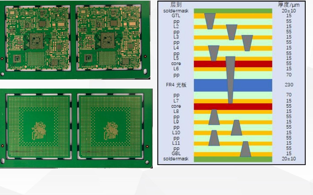
SiP flip-chip substrate
12 layers / 4 stacks, BT (black), 1.20±0.12 mm, unit 55.0×55.0 mm, line/space 40/40 µm, min. bonding 80 µm, OSP finish.

14-layer 6-stack RF substrate
High-speed BT, 1.20±0.12 mm, 190×190 mm, line/space 55/80 µm, immersion silver (non-magnetic process). 6-stack any-layer interconnect with laser drilling + electrolytic via filling.

77 GHz millimeter-wave radar substrate
4 layers / 1 stack, FR4 + Rogers RO3003 hybrid lamination, 0.90±0.09 mm, 31.8×35.2 mm, ENIG + selective OSP.
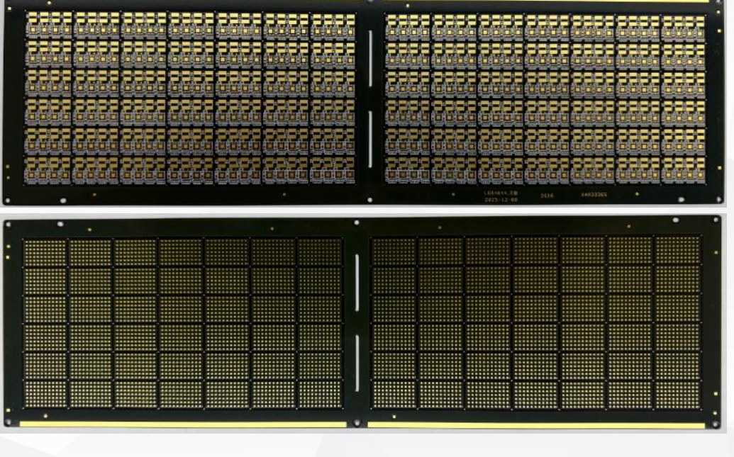
SiP substrate for power devices
4 layers, BT, 0.40±0.04 mm, unit 9.0×15.0 mm, line/space 76/80 µm, nickel-palladium-gold finish. TGV blind vias filled and copper-pillar filling for high-current power-device chips.

eMMC storage substrate
2 / 4 layers, BT, 0.08 mm holes, 0.25±0.02 mm, unit 13.0×11.5 mm, line/space 50/50 µm, min. bonding 55 µm, nickel-palladium-gold finish.

MEMS substrate with built-in cavity
6 layers, BT with built-in cavity and depth-controlled holes, 0.40±0.05 mm, unit 4.72×3.76 mm, nickel-palladium-gold finish.
More production examples
| Type | Layers | Material | Thickness (mm) | Unit size (mm) | Line/Space | Finish |
|---|---|---|---|---|---|---|
| UDP | 2 | FR4 | 0.26±0.02 | 11.3×24.8 | 70/50 µm | ENIG, electrolytic hard Ni-Au |
| T-card / memory card | 2 | BT | 0.26±0.02 | 11.0×15.0 | 50/50 µm | Electrolytic soft Au + hard Ni-Au |
| BGA substrate | 2 | BT | 0.22±0.02 | 12.0×18.0 | 45/50 µm | Electrolytic soft Ni-Au + OSP |
| SiP substrate | 4 | BT | 0.40±0.04 | 9.0×15.0 | 76/80 µm | Ni/Pd/Au |
| LGA package substrate | 4 / 1-stack | BT | 0.20±0.03 | 5.0×5.0 | 65/50 µm | Au/Pd/Au (non-magnetic) |
| 4030 embedded R/C silicon microphone | 4 | Embedded passives material | 0.265±0.05 | 3.0×4.0 | 100/85 µm | Ni/Pd/Au |
| MEMS substrate | 2 | SI10US | 0.20±0.03 | 1.5×1.5 | 70/70 µm | Ni/Pd/Au |
| MEMS substrate | 2 | BT | 0.25±0.05 | 1.85×2.75 | 100/55 µm | Ni/Pd/Au |
| MEMS device substrate | 6 | BT (cavity) | 0.40±0.05 | 4.72×3.76 | 105/60 µm | Ni/Pd/Au |
| PLCC substrate | 4 | BT | 0.30±0.03 | 6.5×6.5 | 100/55 µm | Ni/Pd/Au |
| eMMC storage substrate | 2/4 | BT | 0.25±0.02 | 13.0×11.5 | 50/50 µm | Ni/Pd/Au |
| LED substrate | 2 | BT white | 0.48±0.04 | 0.85×0.85 | 120/60 µm | Electrolytic Ni, Ag |
| MIP 0201/0606 substrate | 2 | BT black/white | 0.14±0.03 | 0.68×0.38 | 120/50 µm | ENIG |
| Laptop substrate | 6 / 1-stack | FR4 | 0.45±0.05 | 98.5×3.06 | 42/60 µm | Ni/Pd/Au |
| 77 GHz mmWave radar | 4 / 1-stack | FR4 + RO3003 hybrid | 0.90±0.09 | 31.8×35.2 | 120/100 µm | ENIG + selective OSP |
| 24 GHz radar | 4 / 1-stack | FR4 + Kappa 438 / RO4350B | 0.80±0.08 | 29.5×41.5 | 150/105 µm | ENIG |
| 24 GHz radar | 4 / 1-stack | S1000-M2 + S7136H hybrid | 0.80±0.08 | 25×25 | 110/100 µm | ENIG |
| UWB radar substrate | 6 / 1-stack | RO4350B + IT180 + F4BM hybrid | 1.60±0.16 | 15.0×44.0 | 150/100 µm | ENIG |
| SiP flip-chip substrate | 12 / 4-stack | BT black | 1.20±0.12 | 55×55 | 40/40 µm | OSP |
| RF substrate | 14 / 6-stack | High-speed BT | 1.20±0.12 | 190×190 | 55/80 µm | Immersion silver (non-magnetic) |
IC Substrate vs. HDI PCB — What’s the Difference?
An HDI PCB connects components on a board; an IC substrate connects a bare die to that board. Substrates work at finer line/space, thinner cores, and tighter registration than board-level HDI, and use substrate-specific materials and finishes. FX PCB manufactures both — see our HDI PCB page for board-level designs.
FAQ
What is an IC substrate PCB?
A packaging substrate that carries a bare IC die and routes its connections out to the PCB, providing electrical connection, protection, and heat paths.
Which materials do you offer?
BT resin (black/white), FR-4, PTFE, BTFE, halogen-free, and high-frequency materials.
Can you handle prototypes?
Yes — HDI samples up to 14 layers / 7 stacks, through-hole samples and production up to 24 layers.
Send us your Gerber files and stack-up for a quote in 1–2 working days. Get a Quote